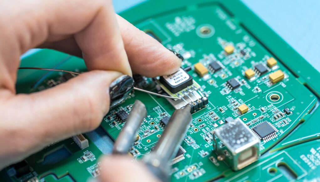
A PCB is a fundamental part of contemporary electronic gadgets and appliances that has transformed the electronics manufacturing sector. Paul Eisler, the PCB’s inventor, used one for the first time in his radio system in 1936, but PCBs didn’t become widely used until the 1950s, when they gradually replaced point-to-point electronic designs.
Table of Contents
Key terminologies for PCB vs. PCB assembly
The term “printed wire card” or “printed wiring board” can also be used to refer to a printed circuit board, abbreviated as PCB. Although it is incorrect, it is also common to see PCBs referred to as PCBAs.
A printed circuit board (PCB) is a blank board with a printed circuit map on it. However, it is not immediately used in electrical devices because it does not have any associated electronic components. It must first go through one of the PCB assembly (PCBA) procedures in order to become a collection of electronic components that can power other electronic products.
Composition of PCB
Depending on the complexity and cost of the finished product, all PCBs are made up of a number of layers of materials. Nevertheless, regardless of these variables, every PCB contains a fundamental substrate layer that supports copper and soldermask layers. These two layers may be found on either one or both sides of the substrate layer.
Fiberglass has long been considered one of the greatest substrates because it gives PCBs the requisite rigidity; yet, some products call for flexible PCBs. High-temperature polymer materials are used to make them.
The following layer is composed of a copper foil that is heated and adhered to the board. The copper layers are typically used to calculate the layers of a PCB. The simplest boards are one layer, however copper can be placed in tens of layers. A layer of soldermask insulates copper to prevent contact with conductive bits or metals.
A layer of silkscreen enables for the labelling of specific PCB components.
Assembly technologies for PCBs
Attaching electronic parts to a PCB’s surface is necessary to transform it into a fully functional device component. This can be accomplished via the more traditional through-hole technology, known as THT, which inserts electronics into holes drilled in the circuit board, or with the more contemporary surface-mount method, also known as SMT. Due to the ability to automate the manufacturing processes, the latter is now increasingly common.
SMT entails using a soldering substance to map the PCB surface. The boards are then sent to a reflow oven for solidifying the solder mask, producing adhesion between a PCB and electronic components, after a pick-and-place machine places each component in its proper location.
How to increase the effectiveness of development
Quartus and ISE’s editing features are inadequate, which reduces the effectiveness of development. Therefore, it is advised to make use of the Sublime text editor’s code fragment feature to lessen repetitious effort. Another widely used simulation tool is Modelsim. To automate the simulation, write your own DO files using TCL/TK.
It is advised to use TCL/TK Introduction Classic as a text. You can manually back up your code, but pros prefer to use Git, a version control system. Another often-used tool is a file comparator called Beyond Compare. Additionally, Git offers a comparison feature. Additionally, System Verilog can be used in place of the testbench and is more effective.
Conclusions
Since a PCB and a PCB assembly are two distinct concepts in electronic manufacturing, understanding the differences between the two is essential for comprehending the fundamentals of PCB assembly. The connections between the electronic components that are adhered to the surface of a PCB using either SMT or through-hole PCB assembly technologies are maintained.


